As VLSI devices shrink to atomic scales, design and analysis become increasingly challenging. Dr. Shahin Nazarian, an expert at Quandary Peak Research and a faculty member in the Electrical Engineering Department at the University of Southern California, has been conducting research on the design and analysis of high speed, energy efficient circuits and systems. He has recently co-authored numerous conference and journal papers in system-level, algorithm-level, device-level, and circuit-level design, analysis and optimization.
More than half a century ago, Gordon Moore predicted that the number of transistors in IC (Integrated Circuit) chips would double roughly every two years[1]. The significance of this prediction is related to the role of transistors as the key logic components in the performance of electronic systems. This prediction, also referred to as Moore’s Law, has sustained its correctness for several decades and has become the primary guidance for the semiconductor community to monitor its long term goals and plans. It is important to note that Moore’s Law is not about the reduction of the size of transistors only, but also cost reduction as well. This implies that design solutions involve high level software and hardware analysis and optimization methodologies in addition to device level techniques.
As the devices have scaled down to 28nm process nodes and below, the traditional bulk CMOS technologies have faced grave challenges linked to device unpredictability and high leakage dissipation induced by short-channel effects and Process-Voltage-Temperature (PVT) variations. There have been massive R&D investments to tackle those issues to help extend Moore’s Law. In parallel, alternative metrics (such as speed per unit power) and laws have emerged as the fear of the end of Moore’s Law grows. One of the most promising solutions has been the adoption of non-planar or quasi-planar FinFET and Gate-All-Around (GAA) transistors that offer more effective channel control, higher ON/OFF current ratios, and superior scalability[2][3].
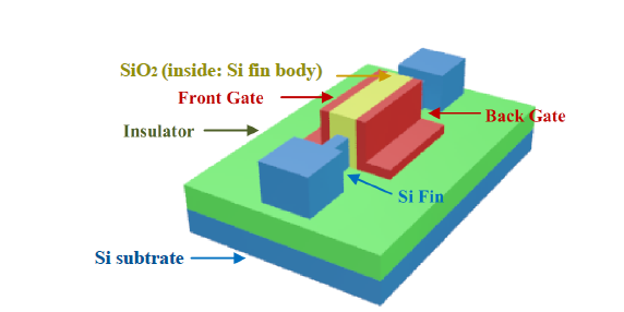
The following figure illustrates an example FinFET transistor with two (back and front) gates, a design which is increasingly used in cutting-edge products. Multi-gate devices are more complex to model and analyze, however. They demand the development of new computer-aided design (CAD) tools, design flows, and platforms in all levels of abstractions and views from system down to the layout.
Efficient Timing Analysis of 6T FinFET SRAMs
Dr. Nazarian and his research team recently analyzed the performance of a 6T FinFET SRAM memory using a 7nm Predictive Technology Model[3]. Timing accuracy is critical in the design of processors and their interactions with cache memories, which are typically fast SRAM memories. A Current Source Model (CSM) is therefore developed for the purpose of static and dynamic timing analysis of SRAMs. Due to the high number of input dependencies, a model based on high-dimensional lookup tables (LUTs) or complex equations would be infeasible. To manage the time/space complexity, they have introduced a model order reduction (MOR) technique based on a “semi-analytical” CSM which allows allows the utilization of low dimensional LUTs and equations.
The following example can be used to capture the basic principle of a semi-analytical model: suppose a current I should relate to three terminal voltages, x, y, and z, based on the following functionality form: I(x, y, z) = f( A(x, y), B(x, z) ). The functional form of this equation is the same for all combinations of the terminal voltages. However, the equation also depends on a set of pre-characterized regression coefficients stored in LUTs, i.e., coefficients A(x, y) and B(x, z) are stored in LUTs corresponding to their (x, y) or (x, z) keys, respectively.
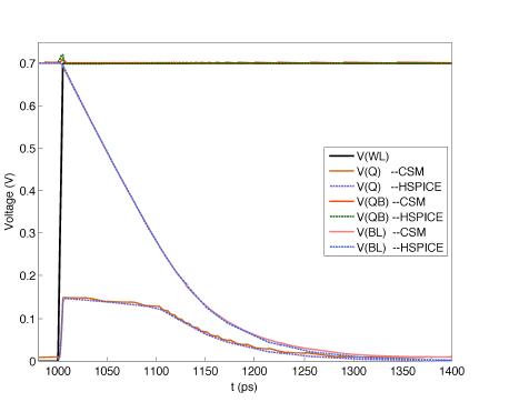
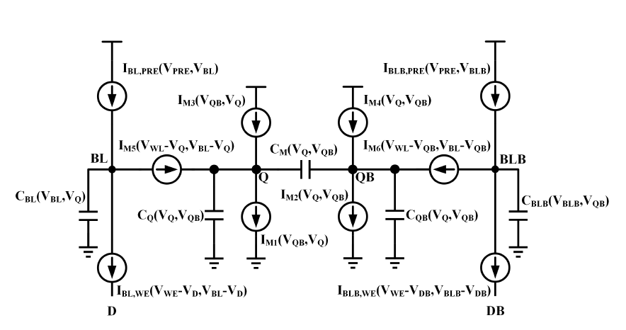
The model order reduction techniques include circuit and analytical techniques. The modified circuit model of one SRAM cell is illustrated in the following figure. Using this circuit model and the reduced semi-analytical functional forms, the space and time complexities of timing calculations are greatly reduced. This has been confirmed using (transistor level) Hspice comparisons.
As an example, timing analysis of a 6T SRAM memory with 512 arrays was measured to have a maximum error of less than 3% while being at least one order of magnitude faster than Hspice. The following figure depicts the actual waveforms during read operations, closely matching their corresponding Hspice versions.